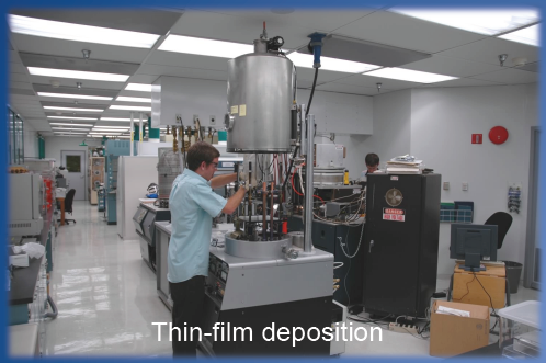
 The Berkeley Lab’s Engineering Division Semiconductor Detector Laboratory provides the infrastructure and expertise for the development and production of semiconductor-based radiation detectors and detection systems. The facility consists of a class 100 clean room, class 10,000 processing and testing area, and a mechanical processing area. We use mechanical and wet chemical processing, thin film deposition, photolithography, wire bonding, and detector characterization to process Ge, CdZnTe, and SI. Several configurations are used including, diffused, implanted, surface barrier, and amorphous contacts, including strip, orthogonal strip, and point contact.
Semiconductor Detector Laboratory
by