
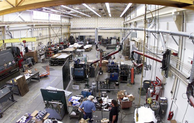
- Location: Building 77
- The Weld Shop employs several different processes to join components together for large and small fabrication projects. The processes include stick welding (SMAW), tungsten torch welding (GTAW), wire feed welding (GMAW), oxy/acetylene, and carbon arc plasma cutting. Typical materials used include steel, stainless steel, and aluminum.


