
Berkeley Lab’s Engineering Division is working on a tiny component that is expected to play a big role in LEGEND-1000, a planned physics project in the Nuclear Science Division. This tiny component—which is currently in research and development—is part of the front-end electronics for LEGEND-1000’s germanium detectors. It is a charge-amplifier application-specific integrated circuit (ASIC), a critical element of the readout electronics system. The ASIC amplifies the charge signals generated when a particle or radiation interacts with a detector, allowing these signals to reach downstream electronics. The ASIC’s performance directly influences the detector’s sensitivity and ability to gather data.
Building sensitive charge amplifiers for particle detectors, particularly in a cryogenic environment, is a specialty area for the Engineering Division’s Electronics, Software, and Instrumentation Department, developed through experience on numerous projects, including the MAJORANA DEMONSTRATOR experiment and the Deep Underground Neutrino Experiment (DUNE).
“The Lab has been designing these cryogenic charge-sensitive amplifiers for many years and for many projects, so we have a lot of experience in that,” explains Marcos Turqueti, Electronic Systems Group Lead and head of development for the ASIC at Berkeley Lab. “And the other critical thing is that it is microelectronics, and it operates at cryogenic temperatures, and that’s a specialized kind of expertise. We do that here in Engineering.”
LEGEND-1000 is designed to study a hypothetical and still unobserved nuclear process called neutrinoless double beta decay. This rare phenomenon is expected to yield important information about fundamental physics questions, such as the origins of mass in the universe and matter-antimatter asymmetry. ASIC development for LEGEND-1000 is a collaboration between teams from the Engineering and Nuclear Science Divisions at Berkeley Lab. LEGEND is a worldwide collaboration, with the US/Department of Energy contribution managed by Oak Ridge National Lab and with ASIC research and development also taking place in Europe.
LEGEND-1000 is still in the development phase, having just undergone Critical Decision 1 (CD-1) review in November 2025. While much of the planning for the project is still ramping up, the engineering research and development effort going into the charge-amplifier ASIC is already in high gear, working to be ready for the down-selection process and then fabrication as detector construction begins. LEGEND-1000 is expected to undergo integration and commissioning in 2038, but in the meantime, there will be an enormous amount of research, engineering, and development going into the project. This shows the effort that goes into discrete components of an instrument of this scale—long before it starts producing scientific data, long before it is installed, and long before all of the pieces are manufactured and assembled.
Electronics in Extreme Environments
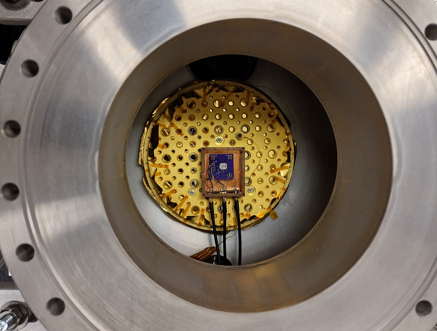
The research and innovation behind the charge-amplifier ASIC being developed for LEGEND-1000 are driven by the experiment’s scientific goals and the demanding conditions of the detector’s extreme operating environment. LEGEND-1000 will consist of nearly 400 detectors made of a germanium isotope, known as 76Ge, which requires extremely cold temperatures to function properly. To keep the germanium cooled, the detectors, along with the preamplifiers, will be immersed in liquid argon to maintain a temperature of 87 K, which is about -300°F. Most electronics, including those intended for industrial applications, will not function below -50°F.
“LEGEND-1000 is a chandelier of detector strings, and on that chandelier, in each string, there are nine germanium detectors, and on top of each detector is one of these ASICs,” explains Alan Poon, a senior scientist at Berkeley Lab who leads the Nuclear Science Division’s LEGEND-1000 efforts. “The detector strings sit in a cryostat tank, and the tank itself is completely filled with liquid argon, and it is large. So, there’s around a five-meter distance between the detectors and the top of the cryostat tank.”
This design makes for a challenging operating environment for electronics, while additional scientific constraints add to the difficulty of constructing an ASIC that will meet the specs and function as needed.
Since each detector has a charge amplifier associated with it, during data collection there will be nearly 400 chips operating at the same time. This has the potential to generate a significant amount of heat, warming the surrounding liquid and causing it to boil off. To combat this issue, the LEGEND-1000 charge amplifier cannot dissipate too much power. The ASIC developed by Berkeley Lab’s Engineering Division uses a small amount of power—operating between 2.5 and 2.8 V helps to limit heat generation.
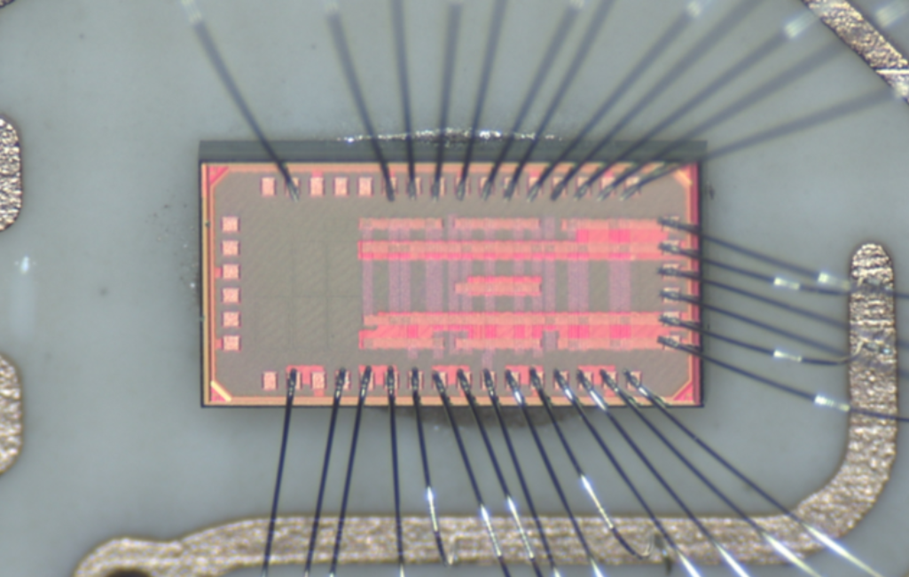
A crucial requirement of LEGEND-1000 is that it must have an extremely low radioactivity background, a key factor in maximizing the detector’s sensitivity and its ability to detect neutrinoless double beta decay. The materials and construction of the detector components are all intended to reduce noise and promote a low-background environment—including the ASIC. LEGEND’s ASIC is a microchip, with external dimensions of 1 mm × 2 mm and a mass of less than 0.5 mg. Reducing the amount of material used in the chip helps to limit interference with the physics signal. Despite its small size, a lot is packed onto the ASIC, including 640 feet of wiring.
“Every material has small traces of radioactivity,” says Turqueti. “All the materials here are processed to remove these tiny bits of radioactive material so that you don’t confuse that radiation with the signal that you actually want to detect. And one of the ways to reduce this radiation is to reduce the amount of material, to make it as small as possible.”
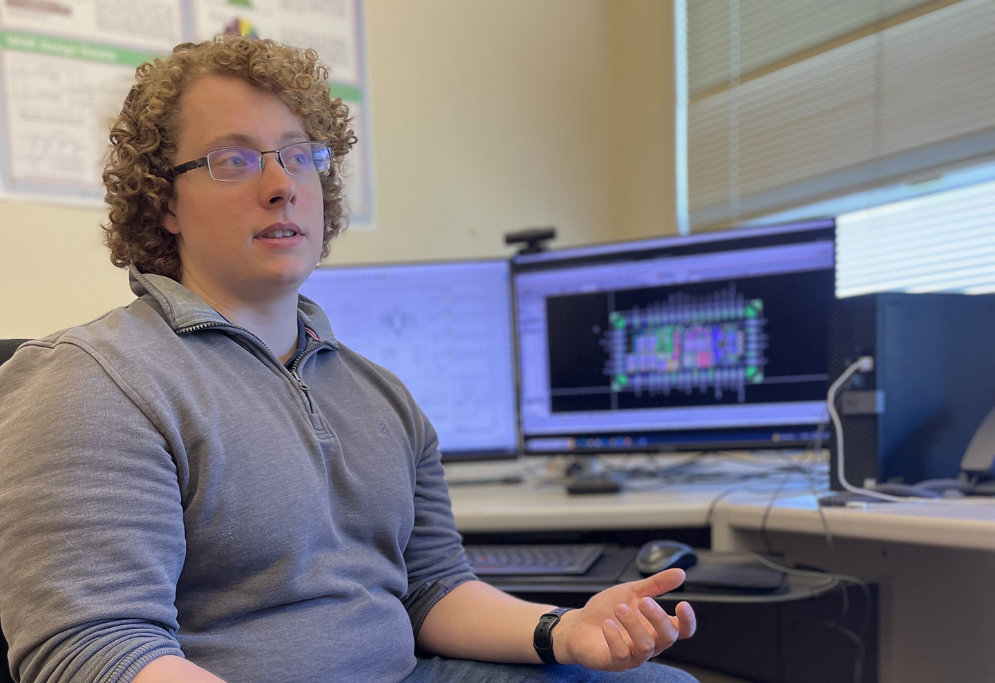
In addition, to minimize radioactive background, the chip was designed as a fully self-contained unit. Unlike a conventional chip, which has external support components like capacitors, this design integrates the necessary elements directly into the chip. Integrated Circuit Design Engineer Will Wright worked to create a voltage regulator design that replaces large external capacitors with small capacitors internal to the ASIC.
“It’s not a trivial matter,” Turqueti clarifies. “Normally, these circuits have large capacitors to store energy, and they work a little bit like a dam. You have a lot of water, and then you just regulate the amount of water using the dam. In this case, we don’t have the dam. We have just a very small reservoir to work with. So, the flow needs to be much, much better regulated.”
Reliability is also an important feature for the charge amplifier, given that it will be submerged in a sealed liquid-argon cryostat with limited ability to perform maintenance or repairs. The charge amplifier must be able to function for at least ten years in these conditions.
Testing, Testing, Testing
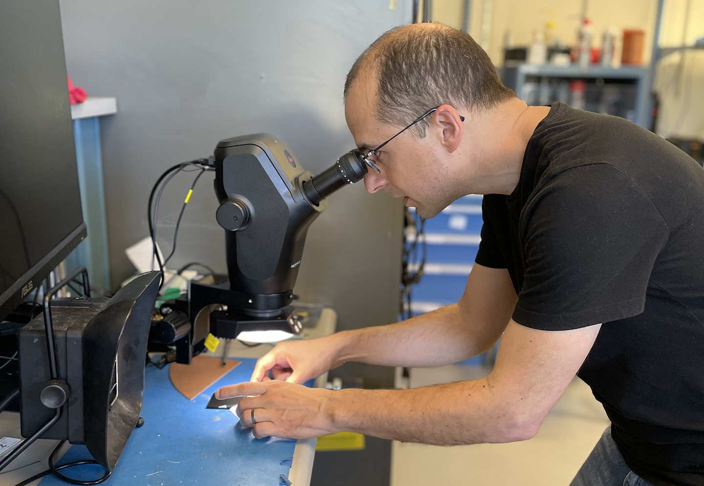
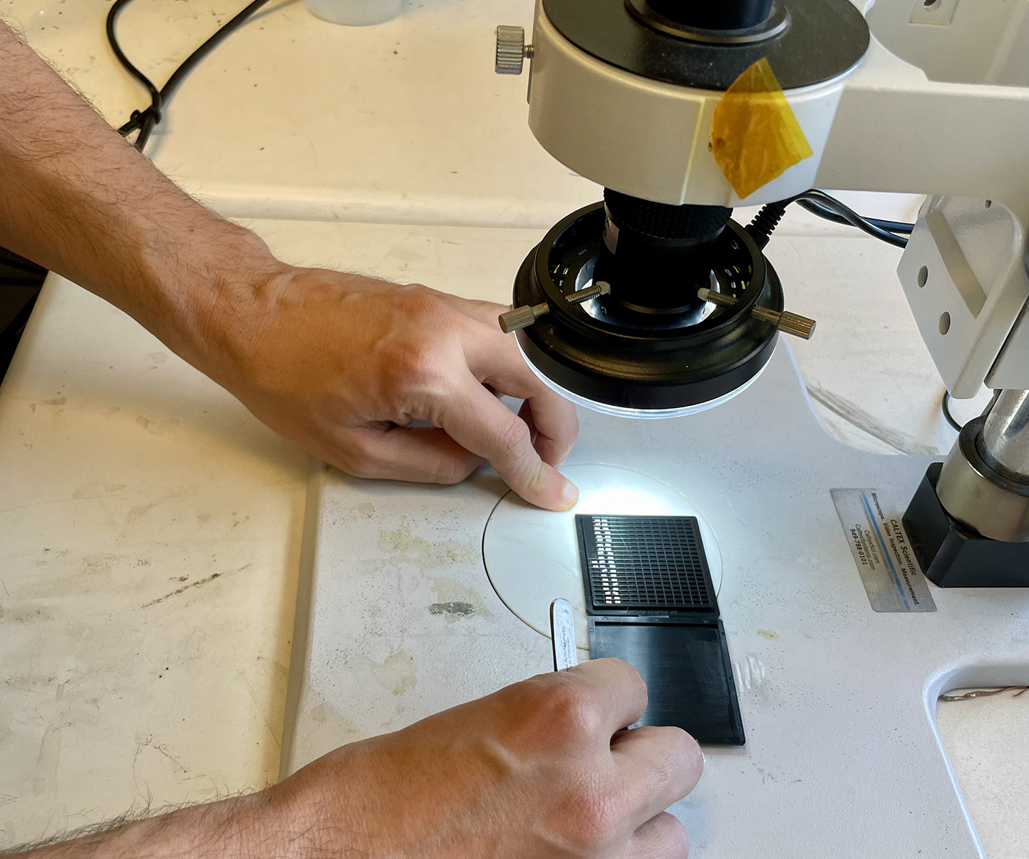
Developing the charge-amplifier ASIC begins with an initial round of modeling and simulations. Following this, a design is created by Turqueti and the team at Berkeley Lab. A specialty manufacturer then makes the prototype ASICs, which are tested at Berkeley Lab. The electronics engineering team then iterates on the next design based on the testing results. Currently, the team is working on the second set of prototypes, with two more rounds planned.
Testing these electronics is a significant challenge.
“The testing of this chip is very involved,” Turqueti comments. “To test these chips is very difficult, and that’s actually sometimes what we spend most of our time on, to make sure it’s compliant with the test.”
Much of the difficulty lies in the fact that the performance of the ASIC is different at warm versus cold temperatures. Because of this difference, the ASIC cannot simply be tested on the bench following the standard procedure for most electronics. Instead, when the chip arrives, preliminary testing is done at room temperature, just to ensure that it is functioning. All other tests are done cold, inside a cryostat that mimics the operating conditions of the detector. If the chip meets the criteria under these conditions, it is then tested with a scaled-down version of the LEGEND detector.
“Just the size of this system is already a challenge,” says Turqueti. “To compact all these components in this tiny piece of silicon and still get something that has such high performance was very difficult. It took years for us to be able to do it, and we are still improving.”
Engineering the Detectors of the Future
The ASIC being developed for LEGEND-1000 by Berkeley Lab’s Engineering Division is one of two efforts to design a charge amplifier for the detector. The other is fielded by colleagues in Europe. A down-selection process will take place further along in LEGEND’s development process.
Berkeley Lab’s Engineering Division will also work on developing, designing, and sourcing the cables that transmit the signals from the ASICs up and out of the liquid-argon cryostat. This effort will be led by electronics engineer Thorsten Stezelberger, who brings experience working on germanium detectors, including GRETA.
For the moment, work continues within the Engineering Division on the charge amplifier ASIC.
“This ASIC is critical because it’s the component that’s closest to the detector,” remarks Poon. “A low-power and radiopure—i.e., low radioactivity—ASIC is the foundation of success for the most sensitive neutrinoless double-beta decay experiment to date, which is what we are aiming to achieve.”
Read a recently published paper that presents findings from testing and characterization of the ASIC here.
