
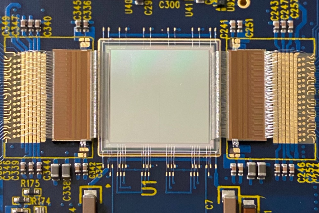
There is a delicate, tiny world in Berkeley Lab’s Engineering Division where highly skilled professionals work with components no bigger than the size of a speck of pollen. This is the world of wire bonding, a specialized process used to connect microchips to their surrounding packaging or to a printed circuit board. At the Lab, wire bonding is a critical capability, instrumental in helping to push science forward on projects like LEGEND 1000, done in collaboration with the Nuclear Science Division, VeryFast CCD, a collaboration with the Advanced Light Source, and the ATLAS upgrade, a collaboration with the Physics Division.
The Engineering Division’s wire bonding experts work on projects that are deemed too challenging by industry or where the quantities are too low to make outside production feasible. Additionally, wire bonding plays an important role in many projects because it provides high performance at a reasonable cost. Wire bonding allows engineers to push technologies to their limits while being cost effective and practical for many science applications at the Lab.
“The challenges are, first, we do crazy stuff,” explains Peter Denes, senior staff scientist at the Molecular Foundry. “So, we do things that are more aggressive than what happens in industry, and typically that means we want very high density so that the wires are all packed very close together, and that makes it just kind of challenging to do wire bonding. We do things that are very much research and development, so you wouldn’t necessarily do them in production. We need these capabilities that are more aggressive than what you would find in industry.”
Denes has worked on many projects that leverage the Engineering Division’s wire bonding capabilities, including VeryFastCCD, an extremely fast X-ray camera that is currently in development.
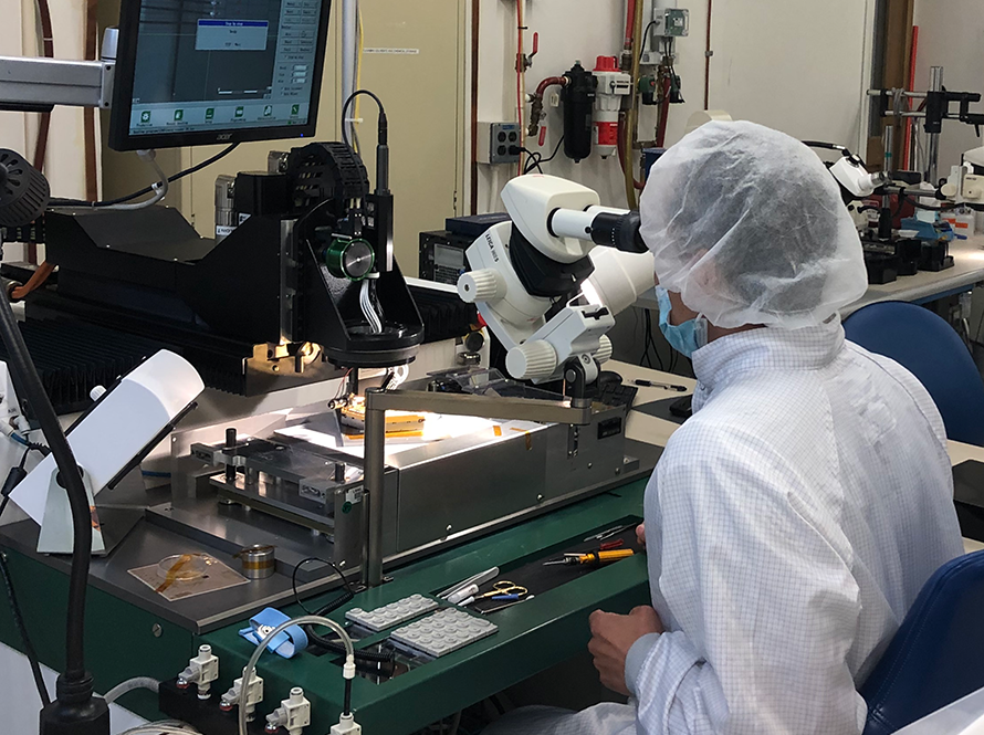
Phathakone Sanethavong working on wire bonding a wafer for a cosmic microwave background project for the Physics Division.
When completed, this camera will take 5,000 pictures per second, a 50-times increase in speed on the current version, known as FastCCD. Denes has worked with Phathakone Sanethavong, a wire bonding expert in the Engineering Division, on a custom integrated circuit that helps convert the signals from the camera into data that can be measured. VeryFastCCD has involved a lot of intense, high-density wire bonding.
This process begins when Denes shares a chip and a wiring diagram with Sanethavong. After a careful examination of the specifications, Sanethavong will write a program for the wire bonding machine telling it where to place and attach each wire to the chip.
Wire bonding in the Engineering Division is done using 25-micron aluminum wire, which the machine attaches to the bond pad on the chip using ultrasonic welding. This process can be relatively straightforward or incredibly challenging depending on the design of the chip and the surface that the wire is being bonded to.
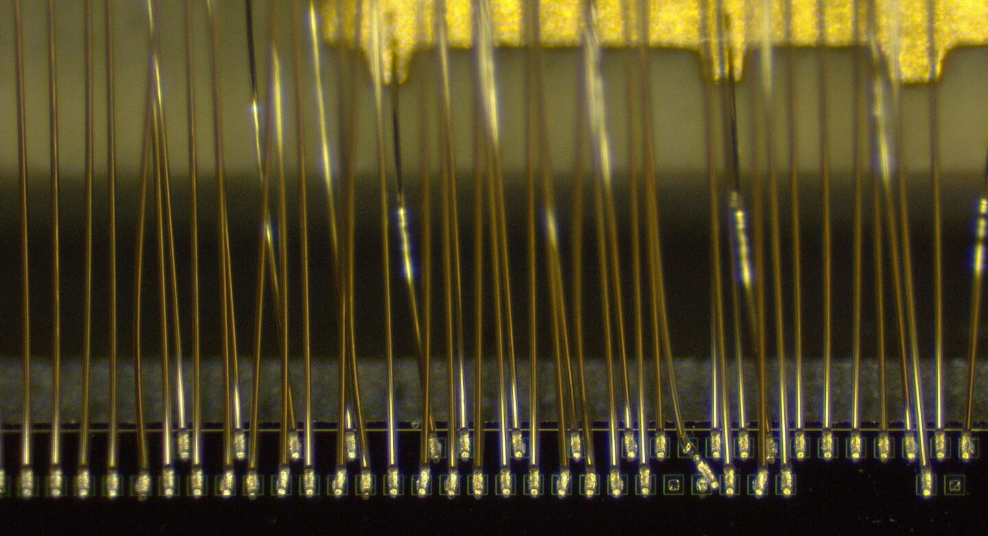
“Some wires can stick really easily; some don’t stick at all,” explains Sanethavong. “It depends on the stability of the substrate that you are bonding and the cleanliness of the surface that you are bonding to. Also, how hard is it? How soft is it? How bouncy? Spongy? Is it glassy? Getting a 25-micron wire to stick to certain surfaces is sometimes very challenging.”
In addition, the design of the chip can have a huge impact on how easy—and fast—the wire bonding job is. For example, jobs with larger bonding pads and larger gaps between the wires are easier to complete. On the other hand, a job where the tolerances are tighter or where the wires pass over each other can be much more challenging.
“I think the smallest bond pads I have ever worked with were for Peter Denes,” says Sanethavong. “A wire is 25 microns. For Peter, and some of his electron microscopy sensors, I had to hit a 30-micron pad, so I had five microns to spare there. And then on top of that, the pads were really close to each other, and the wires cannot be touching each other. So, sometimes you might have to even go in there manually to make sure that nothing is touching. Even though the wire bonding machine will make a perfect bond, the wires will still touch. This is probably one of the most challenging wire bonding projects that I’ve had to do.”
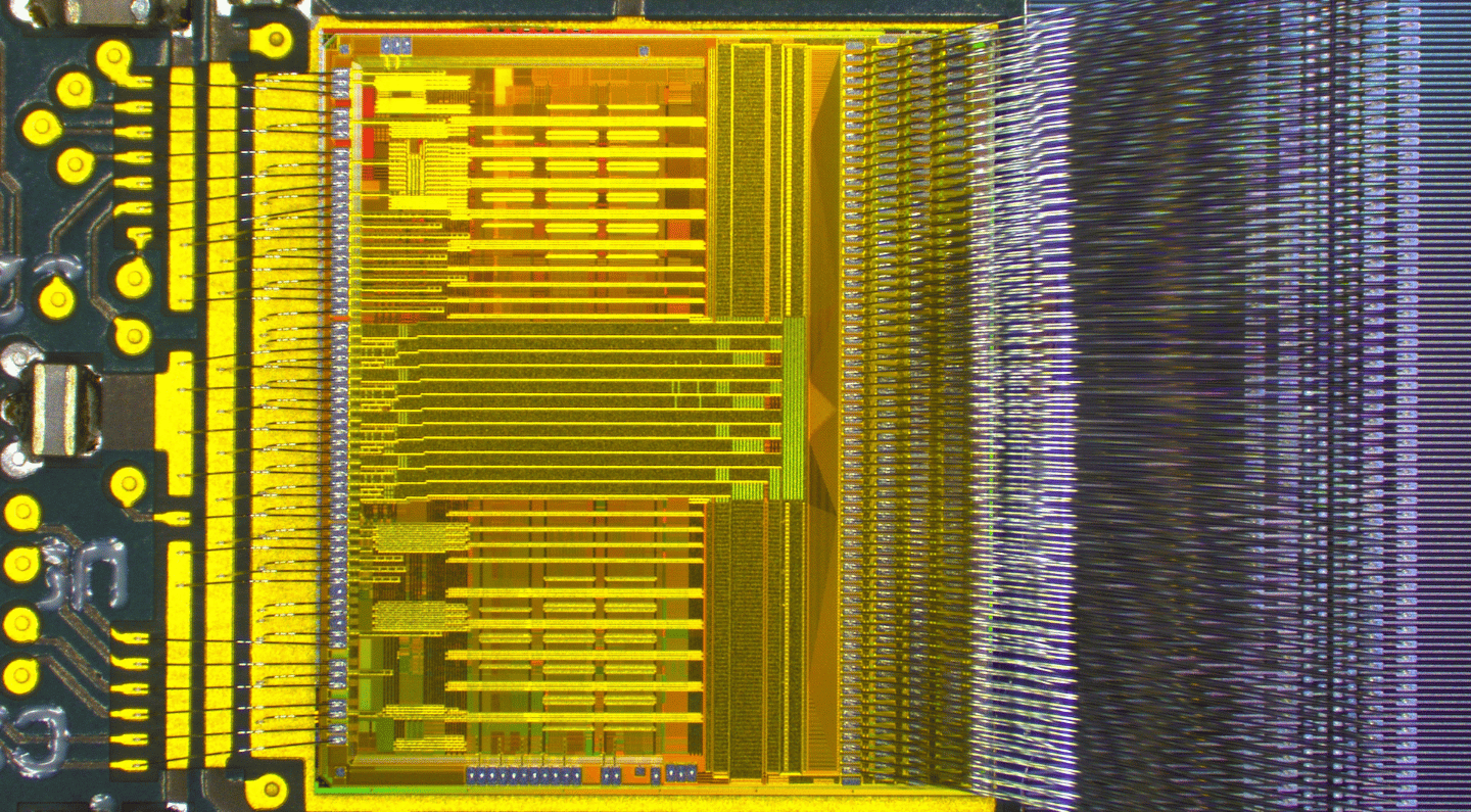
Sanethavong says that in addition to the size and tight tolerances for the electron microscopy sensors, the bond pad is recessed about 15 microns down from the surface, making hitting the pad more important—and more difficult.
The layout of wires on a particular chip can also affect how involved a job is. Each chip for VeryFastCCD has 1,137 individual wires to bond, but because of the configuration of these wires, it takes about a day to complete the wire bonding process for just one chip. As a comparison, for the ATLAS upgrade project Sanethavong is currently working on, each chip has roughly 2,500 wires, yet the configuration is much more straightforward, and one chip takes around an hour and a half to complete.
“High-energy physics relies a lot on application-specific custom integrated circuits (ASICs), designed specifically for our purposes,” says Simone Pagan Griso, senior scientist, Physics Division. “This involves countless hours of prototyping and testing and the in-house wire-bonding is a fundamental skill to be able to accelerate such R&D cycles and bring us to the cutting-edge of research in this domain.”
For many projects like VeryFastCCD, the wire bonding process is a collaborative one that begins in the design phase. Designers will often consult with Sanethavong at this stage for advice on how to make production of the chip feasible.
“The strength of Berkeley Lab, and why we build things here as opposed to just hiring companies to do everything, is because we have situations where, if we really want the best performance for these extreme applications, handcrafting something usually gets you a long way as opposed to just using generic industrial processes,” explains Carl Grace, Electronics, Software, and Instrumentation Engineering Department Head. “We often do strange things, and it’s really helpful for us to have experts who can help us figure out how to do these things. A lot of times it’s not straightforward.”
Sanethavong began his career in the early 2000s, working at HP while he was in college. It was there that he got his first introduction to building things on a small scale, first working on manual wire bonding and then learning to use an auto wire bonding machine. He joined Berkeley Lab’s Engineering Division in 2017.
“It is easy to deal with something that is big, but to control and move something five or 10 microns with your hand and eye, it does take some skill to be able to do that,” Sanethavong says. “But I enjoy doing something that maybe no one else wants to do. To be able to wire bond something for a designer or engineer, to be able to test it, and it works—it is rewarding and challenging to contribute to something like that.”
Made in Berkeley Lab is a series about the many innovative and groundbreaking items the Engineering Division makes on location, showcasing the highly skilled fabrication and manufacturing expertise at the Lab. From tiny robots and tight tolerances to mammoth detectors, powerful magnets, and new materials, it’s all made right here in Berkeley Lab.
